Calibration Wafer Standards
Our Particle Wafer Standards deposited with polystyrene micro-spheres or silica microspheres support Metrology Managers who need to calibrate the size response of their Wafer Inspection Systems and Scanning Surface Inspection Systems (SSIS) and tools with NIST Traceable size accuracy and particle size standards with narrow size distributions.
| Weight | 3 lbs |
|---|
Calibration Wafer Standards are used to calibrate the size accuracy and defect response of Wafer Inspection Systems and Scanning Surface Inspection Systems (SSIS). Wafer Calibration Standards are produced on 300mm, 200mm, 150mm, 100mm, 75mm prime silica wafers, or customer Quartz Masks and customer Film Deposited Wafers. Polystyrene Micro-spheres are the typical particle deposition for low laser power SSIS tools, while Silica Particles are used for Wafer Standards produced to calibrate high power, SSIS tools. These sophisticated wafer inspection tools are provided by manufacturers such as KLA, KLA-Tencor, Hitachi, Applied Materials, Tokyo Electron, etc.
Applied Metrology offers Contamination Wafer Standards and Calibration Wafer Standards, which are also known as Particle Wafer Standards and PSL Wafer Standards. Calibration Wafers are typically deposited with polystyrene microspheres (PSL spheres); while Contamination Wafer Standards are normally deposited with silica micro-spheres. Our wafer standards are deposited on 100mm, 125mm, 150mm, 200mm 300mm wafers as FULL depositions across the wafer standard, or with multiple particle sizes around the wafer standard. Polystyrene microsphere particles and silica microspheres are size standards with NIST Traceable diameter to NIST SRM size standards. Silica microsphere particles are spherical and available from 20 nm to 3000 nm, while polystyrene micro-sphere particles are available from 20 nm to 15 microns. The following is a brief discussion on the use, deposition and applications of Particle Wafer Standards, Contamination Wafer Standards and Calibration Wafer Standards.
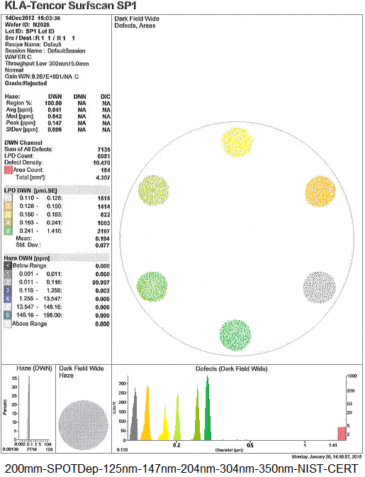
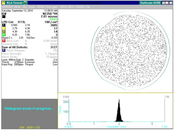
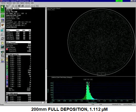
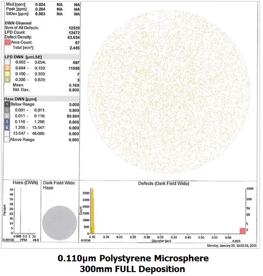
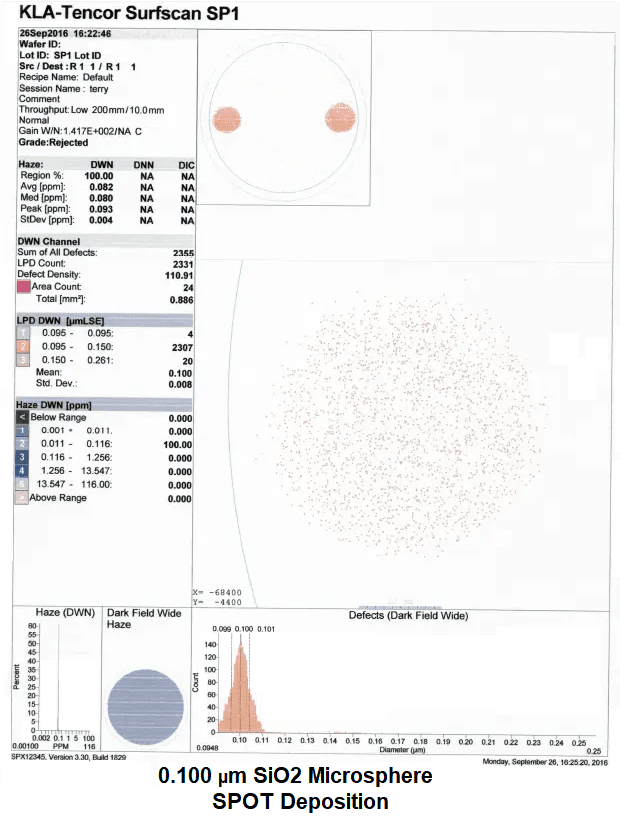
The purpose of Calibration Wafer Standards and Contamination Wafer Standards is to calibrate the size response of wafer inspection tools, such as KLA and KLA-Tencor SP1, SP2, SP3, SP5, SPX SSIS tools; as well as Tencor 6100 and 6200 wafer inspection systems. The industry terms used for these tools is “wafer inspection system” and SSIS, (scanning surface inspection system) tools used to detect surface particles on the silicon wafers and quartz masks. A 300mm or 200mm prime silicon wafer is the typical deposited substrate, but Customer quartz photo masks and glass substrates can also be deposited on. We also provide depositions on customer’s Film Deposited Wafers. Using the silicon wafer as the reference, the wafer is placed in a typical Particle Deposition System, such as the 2300 NPT-1 Particle Deposition System. The 2300 NPT-1 is capable of depositing PSL Spheres and silica micro-spheres on the substrate surface using a Differential Mobility Analyzer (DMA), which isolates a specific particle size peak and isolates the unwanted portion of the background particles. PSL spheres and process particles are directed through the DMA, which uses airflow and electrical charging to pass only a very narrow size peak through the DMA, creating a highly accurate PSL or Silica size peak, which is then counted for approximate count and then deposited as a full deposition of one particle size on the wafer. The 2300 NPT-1 can deposit 1 to 6 NIST Traceable, particle diameters around the wafer surface in one automated step, creating a SPOT Deposition, wafer standard.
Full depositions are traditionally used to calibrate one size point of an SSIS tool, thus as many as 6 full deposition wafers would be used to calibrate the size range of a KLA, KLA-Tencor SP1, SP2, SP3, SPX, Hitachi LS and other wafer inspection tools. The FULL deposition calibration wafer standard allows for the SSIS tool to be calibrated very accurately for particle size response; as well as test the SSIS tool for wafer scan uniformity across the wafer surface. SPOT deposition wafers can also be generated, which can be one to 6 size peaks, deposited around the wafer surface. Thus, when an SSIS tool scans a Spot Deposition Wafer, the SSIS detects multiple size peaks in one scan, and the calibration of the SSIS tool can progress more quickly. SPOT Depositions, as detected by the SSIS tool, are displayed in an X/Y graph, and the SSIS tool can be quickly analyzed for size response across a wide dynamic size range, using one SPOT Deposition Wafer. A FULL deposition, Particle Wafer Standard, has advantages of showing how uniform a wafer inspection tool is during a wafer scan, while a spot deposition wafer can describe any weaknesses of the size response accuracy across a wide size range in one wafer scan.
The more narrow the size peak deposited on the wafer standard is, the more accurate the size response calibration is on the SSIS tool. Polystyrene microspheres are deposited for SSIS tools using a low power laser to scan the Calibration Wafer Standard, whereas Silica micro-spheres are used to deposit Contamination Wafer Standards for SSIS tools using high powered lasers. The Refractive index of silica and polystyrene is very close, allowing for accurate particle size calibration of the SSIS tool using either type of particle.Call Applied Metrology to specify your Wafer Standards on Prime Silica Wafers, or on your quartz masks or your film deposited wafers.
Additional information
| Weight | 3 lbs |
|---|